Better Good Than Lucky
UT’s physicists develop a novel superconductor on a semiconductor platform
Superconductivity in a Hole-Doped Mott-Insulating Triangular Adatom Layer on a Silicon Surface, Physical Review Letters
Authors: Xuefeng Wu, Fangfei Ming, Tyler S. Smith Guowei Liu, Fei Ye, Kedong Wang, Steven Johnston, and Hanno H. Weitering
Imagine the vast array of technological applications for materials that conduct electricity without dissipation energy or heat. Such superconductors exist, but they are typically discovered with blind luck and are only operational at cryogenic temperatures. Researchers at the University of Tennessee, the Southern University of Science and Technology, and Sun Yat-sen University in China have exploited a physical principle underlying high-temperature superconductivity in complex oxide ceramics to construct a novel nanoscale superconductor on a semiconductor platform. By decorating a boron-doped silicon crystal surface with a very dilute amount of tin—equivalent to only one-third atom layer—the team produced single-atom-thick nanoscale superconducting domains with over 100,000 tin atoms. While the superconducting transition temperature is quite low (4.7 Kelvin), there are strong indications that the superconductivity is related to the strongly correlated motion of electrons in the tin layer (so-called ''Mott correlations''). Similar correlations are at play in materials like the cuprates, which would make the newly-discovered tin monolayer system the only known example of correlation-driven superconductivity outside the realm of complex oxide materials. The structural and compositional simplicity of the tin layer offers not only new insights into superconductivity, but also provides means to integrate superconductors with the all-important semiconductor device platform.
Some people, the saying goes, would rather be lucky than good. With results published in Physical Review Letters (PRL), UT’s physicists and their colleagues have shown that creativity and persistence can prove a more rewarding strategy than just waiting on chance. They’ve devised a novel superconductor from the ground up, building on decades’ worth of physics discovery and a base of silicon—a standard of the semiconductor industry. This system is the first example of modifying a conventional semiconductor and creating a superconductor.
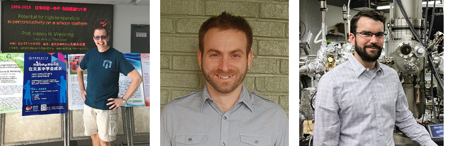
Hanno Weitering, Steve Johnston, and Tyler Smith (L-R) are co-authors on this PRL.
Superconductors pass electrical currents without resistance or giving off heat. Semiconductors dwell somewhere between an ordinary conductor and insulator. Physics Professor and Department Head Hanno Weitering and coworkers came up with the experiment outlined in the PRL paper that brought them together. He explained that “when you have a superconductor and you integrate it with a semiconductor, there are also new types of electronic devices that you can make.”
To arrive at this combination required building on earlier research and then trying something different to see what physics evolved. In the mid-1980s scientists discovered certain materials became superconductors at much higher than typical temperatures. In the years since, physicists have created complex atomic structures that showcase this phenomenon: most made from copper and oxygen (the cuprates). Scientists know that superconductivity results when electrons—which have a natural repulsion toward one another—form pairs. There is no consensus, however, on how they double up in these correlated oxides.
“A superconductor is like a perfect metal,” Weitering explained. “It’s a metal with zero resistance (its magnetic properties, however, are very different from those of a perfect metal). What has to happen for a material to conduct electricity is that the electrons have to hop from one atom to the next; they have to move from one side of the sample to the other side to get a current through.”
The research outlined in PRL indicates compellingly that superconductivity in this case arises from strongly-correlated motion of the electrons of tin atoms placed over a silicon base.
"When you say these are strongly-correlated systems, what we really mean by that are the so-called Mott correlations," Weitering said. "Mott correlations essentially tell these electrons to stay at home, on their own atom. Don’t visit your neighbor. That’s because these electrons repel each other so strongly when they are sitting on the same atom. A Mott insulator is essentially the stay-at-home condition for electrons. To move to your neighbor, let alone move across the whole crystal, costs too much energy. The remarkable thing is that if you dope a Mott insulator, meaning that you insert a few ‘foreign atoms’ (in this case by inserting boron atoms below the tin layer), you create holes in the electron system and electrons start moving again."
This is essentially taking out a small fraction of electrons, leaving spaces for neighboring electrons to move into. Those electrons leave holes behind, so other electrons can make the jump, and then additional electrons can jump, so eventually you can make a conductor. To make it a superconductor, however, the electrons have to move in pairs, and for them to do so, Weitering said, "you need a strong glue to pair them up."
In a conventional superconductor, that glue is provided by the lattice—the repetitive pattern of atoms in a crystalline material. If an electron zips by an atom, it deforms the lattice and through that deformation it pulls in another electron, forming a pair. In an unconventional superconductor, the typical explanation is that fluctuations in magnetism provide the glue to pair two electrons. Weitering said one of the biggest surprises of the doped tin system was that it exhibits much of the same physics learned from studying more complex high-temperature superconductors, which are unconventional.
"We do not know yet whether the pairing mechanism in the tin layer is indeed unconventional, but in all likelihood it is, as Mott correlations tend to suppress conventional pairing," Weitering said.
It’s also a much simpler system, compatible with a semiconductor, because it uses tin.
Tin is in the same column of the periodic table as silicon, just two squares down, and has the same kind of bonding geometry. Lead and germanium live here too, but only tin or lead will work with silicon to make the desired structure. Tin, however, makes everything so much simpler.
"This is likely an unconventional superconductor, and this is why we were pursuing this," Weitering said. "If you look at unconventional superconductors that have been discovered, these are compounds that are chemically very complex. It’s usually a mixture of three, four, of five different elements. These are very complicated materials. Silicon is so simple, and then tin is almost like silicon, so it’s a really simple structure."
Associate Professor Steve Johnston, another of the paper's authors, added, "It’s a theorists dream! This system will allow you to study unconventional superconductivity without any of the usual complications that arise when studying complex oxides."
The system is so simple, in fact, that the experiment called for only one-third of a layer of tin atoms to "decorate" the silicon surface. Imagine a layer of nine billiard balls, with each representing a silicon atom. Then add a second layer of billiard balls on top, but only three instead of nine, as far apart as possible. That’s one-third of a layer. Weitering describes it as "distributing some pearls" on the surface.
The experiment showed superconductivity across a domain of about 100,000 tin atoms, with an area measuring .2 x .2 microns. (To put this in perspective, a human hair is roughly 100 microns in diameter.)
"No one has ever actually done any such kind of modification of a semiconductor surface and created a superconductor," Weitering said. "It’s never been done."
But discoveries like this don’t happen overnight, and for Weitering it was a long journey.
In 1996 Weitering and his mentor, the late Ward Plummer, published results in Nature showing they had discovered a surface charge density wave on a lead-coated germanium crystal. This work lasted until the early 2000s, when both went on to other studies. European colleagues, however, had funding to stay the course, and eventually came around to trying out tin on silicon. They didn’t see a charge density wave, so they presumed they were looking at a Mott insulator.
Inspired, Weitering wrote a proposal to the National Science Foundation in 2013, together with former Oak Ridge National Laboratory collaborator Paul Snijders, proposing that if you dope this new Mott insulator you just might see the same physics as you did with the cuprates—superconductivity—and it could be done on a silicon platform. It was not an intuitive proposition to many because in bulk form, tin and silicon are considered to be weakly correlated, a far cry from the strong Mott correlations they were after. Bulk tin becomes superconducting below 3.7 Kelvin. It is a conventional superconductor and altogether a very different materials system.
In 2017 his research group (including PRL co-author Fangfei Ming, now at Sun Yat-sen University in China, and Johnston) published results showing the system was indeed a Mott insulator and doping it mimicked cuprate physics. This year, using the ultralow-temperature scanning tunneling microscope at Professor Kedong Wang’s lab in China, Ming and his coworkers showed that superconductivity was there, though it vanishes at 4.7 Kelvin. Graduate student (and 2020 PhD alumnus) Tyler Smith travelled to China to work on the study, and Johnston helped provide theoretical framework. Both are co-authors on the PRL paper.
"Usually superconductors are discovered by accident," Weitering said. "Yet this entire approach—doping a Mott insulator, the tin on silicon—was a deliberate strategy. (Then) came proving we’re seeing the properties of a doped Mott insulator as opposed to anything else (and) ruling out other interpretations. The next logical step was demonstrating superconductivity, and lo and behold, it worked."
Combining superconductivity and semiconductors could—way in the future—lead to very fast, highly sensitive, low-loss quantum devices. And using silicon saves a crucial step.
"Anything you can do on a silicon platform potentially has a huge advantage," Weitering said. "The whole microelectronics industry—everything that’s in your smartphone or in your computer—is based on silicon."
To create something based on a totally new material system, he added, would mean setting up completely new fabrication lines. With silicon, the whole industry platform is already in place.
Traditional high-temperature superconducting materials—the metal oxides—don’t have the same possibility for the electronics industry. But without them, scientists wouldn’t have known definitively what they discovered with this new superconductor. Considering room temperature is 293 Kelvin, getting superconductivity at 4.7 Kelvin might not seem particularly impressive at first, but for scientists like Weitering and his colleagues, these results build on the past to help create a future with ever-expanding possibilities.
"Don’t expect any immediate application," Weitering said. "The important thing is that we established a proof of principle."
Drawing inspiration once again from the cuprates, he is now looking for ways to increase the superconducting transition temperature. The cuprates show superconductivity at much higher temperatures, but typically have a square lattice structure, whereas the tin layer is triangular.
"For my next proposal what I’d like to do is see if I can identify systems or if I can play the same trick on the square lattice," he said. "If we can realize a significant increase in superconducting temperature using plain silicon, then that would be the realization of a long-held dream."
The results of this work are published in "Superconductivity in a Hole-Doped Mott-Insulating Triangular Adatom Layer on a Silicon Surface." The milli-Kelvin STM experiment was conducted by Weitering’s former postdoc Dr. Fangfei Ming and his new coworkers in Shenzhen, China. Tyler Smith photo credit: UT Office of Research and Engagement.